
Witaj!
Blog archiwalny. Już niebawem nowy serwis!
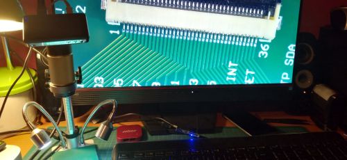 Cyfrowy mikroskop Andonstar ADSM201
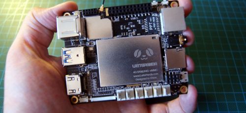 LattePanda z procesorem Intel Atom x5 Z8300
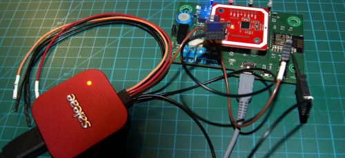 Wybieramy analizator stanów logicznych
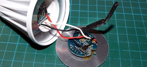 Komunikacja Wi-Fi z żarówką RGB od ChiChinLighting
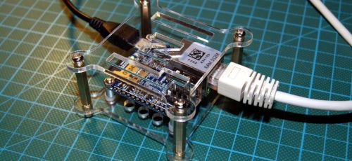 NanoPi NEO - miniaturowy Allwinner H3 za bezcen
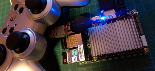
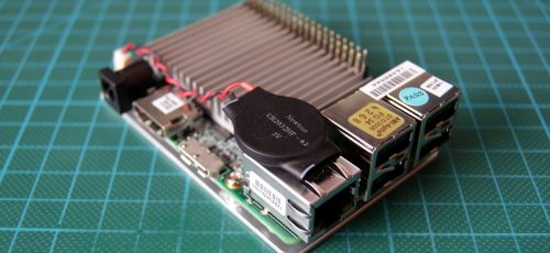
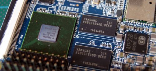 NanoPI M3 - ośmiordzeniowec z układem Samsung S5P6818
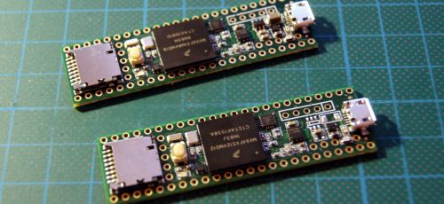 Pierwsze spojrzenie na nowe Teensy 3.5 i Teensy 3.6
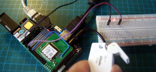 Inteligentny dom z czujnikami EnOcean i Up-Board
 Jak sprawuje się Up Board pod Linuksem?
 Up Board - SBC z procesorem Intel Atom x5 Z8350
Capable of driving panels with resolutions of 1366x768 or 1920x1080 .
Schematic diagrams are the blueprints of electronic devices, offering a visual representation of the components, their connections, and the overall circuitry. For Tp.v56.pb801, having access to a schematic diagram in PDF format can be incredibly valuable for several reasons:
Before studying the schematic, understand the major zones on the physical board:
: Websites specializing in technical documentation, such as Datasheet catalogs or document archives, might host the Tp.v56.pb801 schematic diagram in PDF format.
: The first point of contact should be the official website of the component or device manufacturer. Many companies provide technical documentation, including schematic diagrams, for their products.
: When dealing with faulty devices, a schematic diagram is indispensable for identifying the problematic components and tracing the signal flow. This accelerates the repair process and reduces the risk of further damage.
Controlled by the triple 1118 combo regulator IC . A common fault occurs when the 3.3V supply drops (e.g., to 2.7V) upon releasing standby, indicating the regulator cannot handle the load.
Disclaimer: Always disconnect AC power before probing. High voltages (>300V) persist on primary capacitors even after unplugging. Discharge via a 10k/5W resistor before servicing.
A typical is organized into several pages. Here is what each page contains and how to interpret it:
Without the PDF, you would have spent hours guessing.

2012: lis |
gru |
2013: sty |
lut |
mar |
kwi |
maj |
cze |
lip |
sie |
wrz |
paź |
lis |
gru |
2014: sty |
lut |
mar |
kwi |
maj |
cze |
lip |
sie |
paź |
lis |
gru |
2015: sty |
lut |
mar |
kwi |
maj |
cze |
lip |
2016: sty |
lut |
mar |
kwi |
wrz |
paź |
2017: sty |
lut |
mar |
lip |

